UV Laser Shutters For Semiconductor Manufacturing Processes

A high-precision UV laser shutter for semiconductor manufacturing functions as a timing control that supports accurate wafer processes and long-term reliability. Facilities depend on consistent beam modulation for pattern formation, inspection, and micro-scale adjustments.
A reliable shutter contributes to predictable exposure windows that help maintain uniform structures across each production cycle. Modern semiconductor tools operate within extremely tight tolerances, so steady shutter performance supports the rhythm of the entire process.
Production teams rely on repeatable beam accuracy since even slight timing shifts can influence pattern depth or edge definition. A stable shutter helps maintain that consistency across long service windows. This supports equipment uptime and protects delicate fabrication stages from exposure to irregularities.
Why UV Laser Control Matters In Semiconductor Workflow
Semiconductor equipment handles jobs that call for short pulses, fine beam alignment, and repeatable movement. UV wavelengths often appear in photolithography, inspection, micro-machining, marking, and metrology.
Each task places specific demands on timing. A shutter regulates that exposure and creates predictable openings for the beam so the equipment maintains proper process timing. Modern systems run continuous production for extended periods. Any tool involved in those timelines must be capable of cycling repeatedly without performance drift.
UV shutters contribute to that rhythm since the opening and closing speed shapes every beam interaction. Consistency in those movements supports predictable energy delivery during delicate wafer work.
Why UV Shutters Matter In Fabrication
UV shutters influence more than momentary beam interruption. They support alignment phases, calibration cycles, and fine patterning. During exposure steps, a shutter prevents stray light from striking the wafer before the system is ready.
During calibration, a shutter allows technicians to adjust intensity and focus without affecting nearby surfaces. Each small action contributes to a larger patterning process grounded in stability.
UV systems commonly run at high cycle rates. A shutter built for longevity avoids performance fatigue as exposure counts rise.
That reliability protects equipment timing across thousands of operational hours. For facilities that manage complex wafer mixtures, this type of consistency delivers repeatable outcomes from shift to shift.
How UV Laser Shutters Support Clean Room Expectations
Clean rooms limit contamination, vibration, and external interference. A shutter must operate quietly, smoothly, and consistently so the tool can perform without introducing unnecessary movement.
Stable mechanical action contributes to predictable exposure windows during photolithography or metrology.
A well-designed shutter helps protect internal equipment components from scatter and stray reflections. Precise actuation supports cleaner machine output. This complements the design goals of many semiconductor tools.
Using UV Laser Shutters In Multiple Fabrication Stages
Semiconductor plants often run a mix of UV, visible, excimer, X-ray, and other specialized systems. UV shutters usually operate in photolithography setups that pattern wafer surfaces. They also appear in inspection stations that use short wavelengths to evaluate fine structures.
An X-ray laser shutter supports different wavelengths and different mechanical timings. Although the application differs, the concept remains the same since precise energy control protects the wafer’s structural accuracy.
Many plants use several shutter types across their tool lineup. Each one does a distinct job connected to exposure timing and pattern fidelity.
Custom Solutions For Specialized Equipment
Some semiconductor machines operate in extremely narrow tolerance windows, so a standard shutter might not match those requirements. A custom laser shutter allows engineers to choose the timing profile, stroke length, size, speed, and mounting layout to match their tool. This approach promotes stable performance because the shutter is built for the specific energy profile and optical path involved.
Custom designs are also valuable for legacy systems. Many fabrication plants continue to use long-running equipment that stays dependable but needs refreshed shutter components. Customized parts can match the original layout and system geometry, which lets technicians maintain the tool without taking on large-scale redesign work.
How UV Shutters Compare To Other Beam Control Tools
Clean rooms limit contamination, vibration, and unwanted environmental influence. A system that uses UV laser shutters benefits from stable mechanical motion that supports predictable exposure windows during photolithography or metrology. The controlled action helps protect nearby components from stray reflections since the shutter opens and closes with consistent timing.
Smooth operation supports cleaner machine output. This contributes to accurate pattern development and dependable wafer inspection throughout long production cycles. The broader category of laser shutters and optical beam shutters includes a number of designs. Each target has different power levels, cycle speeds, or wavelengths.
UV shutters sit in that family but stand apart because semiconductors demand tight wavelength control. Fine timing at UV wavelengths helps maintain pattern sharpness during wafer creation.
Modern Semiconductor Plants Depend On Lifetime Performance
Tools inside a semiconductor plant face long service windows. A shutter must maintain reliable timing from installation forward. Lifetime performance supports production goals and protects yield rates from exposure irregularities. High-quality shutters contribute to uptime, so equipment operators avoid timing drift and interruptions.
Predictable mechanical stability helps safeguard both the machine and the wafer. A shutter that moves in a stable, repeatable arc supports consistent exposure cycles hour after hour.
The fabrication line benefits from that reliability because sensitive wafer structures depend on predictable UV intervals.
How We Support Semiconductor Teams At NM Laser Products
NM Laser Products approaches every project with a commitment to longevity and repeatable performance. Our UV shutters are made in the United States and each one passes through controlled manufacturing steps that support timing accuracy and smooth motion.
We track performance across long cycle counts so our designs stay dependable for semiconductor teams that require predictable output from their tools.
Our focus on quality helps extend equipment uptime and strengthens overall process stability for the facilities that use our shutters.
Our engineers have more than three decades of experience designing high-reliability beam control hardware. That history shapes every shutter we build since semiconductor tools call for dependable speed and consistent mechanical action.
When a project demands a specialized footprint or timing profile, we develop customized shutter designs that match those operational needs.
Our goal is simple: Support semiconductor workflows with products that contribute to accurate beam control from installation through long-term operation.
If you have any questions about NM Laser Products, feel free to contact us.
Related Blogs

The Truth About Laser Beam Security Systems
Quick Summary Laser beam security systems are widely misunderstood...
Read more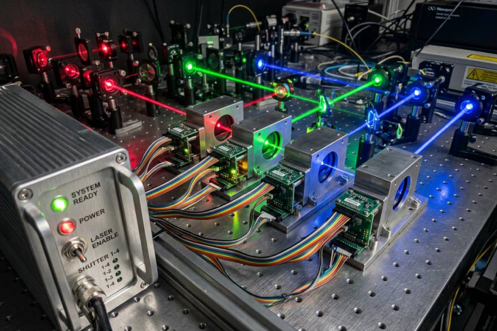
Insights On Laser Shutter Controllers: What To Know
Quick Summary A laser shutter controller does more than simply ope...
Read more
How Lasers Are Classified In Modern Technology
Quick Summary Laser classification is the foundation of laser safe...
Read more